
What is thick film printing?
Thick Film Printing
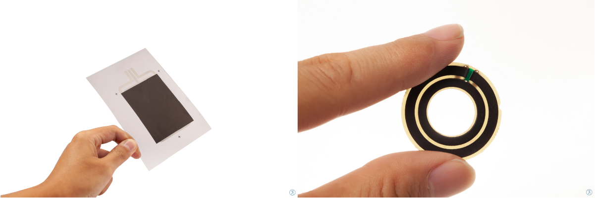
Currently, this technology has matured significantly and can be printed on various substrates, from high-temperature ceramics to common FR4 materials, or polyimide (PI) flexible materials. The resistance can range from 10 ohms/square to 100K ohms/square (resistance value), with a maximum resistance value of up to 100M ohms and a tolerance of +/-10%.Thick Film PrintingPrinted on the etched copper outer layer, and cured in a standard convection oven, infrared oven, or hot air oven, followed by laser trimming to adjust resistance for tight tolerances.
This Thick Film PrintingThe solution makes the resistors embedded in printed circuit boards more complex, but more versatile than choosing surface-mounted passive components. This frees up surface space for placing more active components, thereby increasing functionality.
Thick Film PrintingBy eliminating the need for special terminal treatments, such as immersion silver or silver-palladium, the process of embedded resistors has been improved, and the laser trimming process has been accelerated with tighter TCR; reliability performance has been enhanced through a stable adhesive system. On the other hand, currently available for testing isThick Film PrintingThe values show good adhesion to clean copper surfaces. This eliminates the need for silver immersion or silver-palladium, and gold-palladium saves costs while reducing concerns about silver migration.
Thick Film PrintingThe technology can be used to combine fixed resistors, switches, sensors, sliding potentiometers, and any combination of conductors onto any size and shape of PCB style.